The 8031 reset circuit is perhaps the single most important circuit in the QuadraVerb. When this circuit is functioning incorrectly, problems ranging from loss of battery backup, to a complete lock-up of the machine, can occur. A thorough knowledge of the operation of this circuit will greatly facilitate troubleshooting this unit.
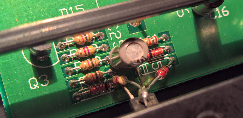
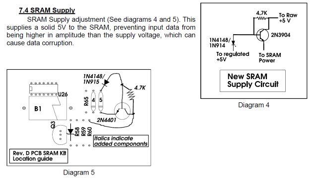
This circuit uses the differential between raw +10V, and regulated +5V, to generate the required signals for system reset. This is necessary due to fact that the system MUST be in a reset state while powering down, otherwise, random noise on the 8031 data, and address, busses could corrupt SRAM data, and destroy any hope that the battery backup will work. C25 acts as a long time constant, to ensure that reset line is enabled long enough for proper system reset. D7 acts as a quick discharge path for C25, ensuring that resets will occur, even if the unit is turned off, and then rapidly back on. R16, R60, R58, and D15, work together as a voltage divider to the base of Q3, and is designed so that transistor Q3 will turn on when the raw +10V supply is roughly 7V. This is to ensure that reset does not occur until after the +5V regulator is fully functioning (i.e. +5V rail is solid). If reset occurs too early, noise on the +5V rail can cause data corruption. Pull-up resistor R59 holds the input of the inverter (U25, pins 13, 12) high, until Q3 turns on, pulling the input low. When this occurs, the output of 2nd inverter (U25 pins 10, 11) will also go low, slowly, due to the time constant of R95, and C32. The power off reset is similar. When the +10V raw supply sinks below 7V, Q3 is turned off, allowing the input of the inverter (U25, pins 13,12) to pull high (via pull-up R59), and thus the same for the output of the 2nd inverter (U25, pins 10,11). Also note the tap between the two inverters, running to the input of AND gate U26 (pins 1,2, and 3). This prevents access to SRAM functions while in the reset condition, thus preventing data corruption.
